In [1]:


from IPython.core.display import HTML
HTML(open('../css/custom.css', 'r').read())
Out[1]:
Note: If you're reading this as a static HTML page, you can also get it as an executable Jupyter notebook here.
Those are big, scary words often associated with FPGA designs, but with simple meanings:
Hierarchy: "See that big, complex thing? It's actually made of small, simple things. And those small, simple things are made of even smaller, simpler things."
Abstraction: "See that thing? It does something. I don't care how it does it. I just need to know what it does."
Ursidae: This is the scientific family name for bears. They have nothing to do with this chapter. I just needed it to make the whole Wizard of Oz reference work.
Take a car as an example. It consists of a body and a drive train. The drive train is made up of an engine, transmission, drive shaft, axles and wheels. And the engine is made up of a block, pistons, fuel injectors, etc. And on and on. That's hierarchy.
Then think about somebody who's putting an engine in a car. He needs to know how big the engine is, how to feed gas to it, and where the spinny thing is that attaches to the drive shaft and makes the wheels go round. All the stuff about piston rings and camshafts and coolant channels are details he can ignore. That's abstraction.
And what about Ursidae? Bears have nothing to do with this. I told you that already. Just let it go.
The role of hierarchy and abstraction in digital design is best understood by going through a concrete example. And what's the best example we have at this point?
Let's rebuild the LED blinker from our previous example as a hierarchy of smaller pieces of digital logic. I'll do this in two phases:
This process - break it down starting from the top, then rebuild it starting from the bottom - is a common technique used in software design. Since building hardware using an HDL is similar to writing software, it's no surprise the pattern works here.
Let's start by showing the LED blinker at it's highest level of abstraction: it takes a clock as input and generates a single output that turns an LED on and off:
At the next level of abstraction, we already know the blinker is built from an $N$-bit counter with the LED output driven from the counter's MSB.
Going down another level, a counter can be constructed from an $N$-bit register and an $N$-bit binary adder). The register holds a value $V$ and, on every pulse of the clock input, that value is replaced by $V + 1$.
The register consists of $N$ individual D flip-flops each of which stores a single bit of the register value that is updated when there is a rising edge of the clock input:
The adder is also composed of $N$ subcomponents called
full-adder bits.
The $k$-th full-adder bit takes the $k$-th bit from each of the numbers to be added along with
a carry bit from the preceding stage of the adder.
It combines these to compute the $k$-th sum bit and a carry bit for the next stage of the adder.
In the figure below, I've replaced the a input with the value 0...001 because the
adder is being used to increment the value on the b input.
I've also placed a 0 on the carry input into the first bit of the adder.
Finally, each full-adder bit is built from a collection of primitive logic gates [1] like this:
And that's the complete breakdown of the LED blinker. Now it's time to build it back up using MyHDL.
I broke the LED blinker down to its most basic components, now I'll start at the lowest level of the hierarchy to build it back up.
Here's the MyHDL code for a single D flip-flop. It's a simple piece of sequential logic that copies its input to its output whenever there is a rising edge on the clock input:
In [2]:


from pygmyhdl import *

@chunk
def dff(clk_i, d_i, q_o):
    '''
    Inputs:
      clk_i: Rising edge on this input stores data on d_i into q_o.
      d_i: Input that brings new data into the flip-flop:
    Outputs:
      q_o: Output of the data stored in the flip-flop.
    '''
    @seq_logic(clk_i.posedge)
    def logic():
        q_o.next = d_i
Now I can build a register by instantiating multiple dff modules in a loop:
In [3]:


@chunk
def register(clk_i, d_i, q_o):
    for k in range(len(d_i)):
        dff(clk_i, d_i.o[k], q_o.i[k])
The loop count is set by the number of bits in the incoming data bus, d_i.
During each loop iteration, a D flip-flop is created.
The d_i.o[k] notation [2] says that the $k$-th output bit of
the d_i bus is used to drive the data input of the $k$-th flip-flop.
In a similar manner, the q_o.i[k] notation says that the output of the $k$-th
flip-flop will drive the $k$-th input bit of the q_o bus.
In this way, the register input bus is applied to the individual flip-flops, and the
flip-flop outputs collectively drive the register output bus.
To test the register, I'll connect it to a clock signal and some input and output buses [3]. Then, I'll use a simple test bench function to apply random values to the register input and see if those values propagate to the register output:
In [4]:


initialize()  # Initialize for simulation.

# Create clock signal and 8-bit register input and output buses.
clk = Wire(name='clk')
data_in = Bus(8, name='data_in')
data_out = Bus(8, name='data_out')

# Instantiate a register and attach the clock and I/O buses.
register(clk_i=clk, d_i=data_in, q_o=data_out)

# Apply random 8-bit integers to the register input along with
# rising and falling edges of the clock signal.
from random import randint  # Random integer function.
def test_bench():
    # Apply ten random inputs to the register.
    for i in range(10):
        data_in.next = randint(0,256)  # Set register input to a random 8-bit value.
        clk.next = 0  # Lower clock signal to 0.
        yield delay(1)  # Wait for one unit of simulation time.
        clk.next = 1  # Then raise the clock signal to 1 ...
        yield delay(1)  # ... and wait one more time unit. The register output should change.

# Pass the test bench function to the simulator function to run the simulation.
simulate(test_bench())

# View the results of the simulation.
show_waveforms()
From the logic waveforms, you can see the value on the data_in bus is transferred to the
data_out bus whenever a rising edge occurs on the clk signal.
The register appears to be working, so I'll move on to begin implementing the adder branch of the blinker hierarchy. Here's the MyHDL for the combinatorial logic of a single full-adder bit:
In [5]:


@chunk
def full_adder_bit(a_i, b_i, c_i, s_o, c_o):
    '''
    Inputs:
      a_i, b_i: Inputs from i-th bit of a and b values.
      c_i: Input from carry output of (i-1)-th adder stage.
    Outputs:
      s_o: Output of i-th sum bit.
      c_o: Carry output to the (i+1)-th adder stage.
    '''
    @comb_logic
    def logic():
        # Exclusive-OR (^) the inputs to create the sum bit.
        s_o.next = a_i ^ b_i ^ c_i
        # Generate a carry output if two or more of the inputs are 1.
        # This uses the logic AND (&) and OR (|) operators.
        c_o.next = (a_i & b_i) | (a_i & c_i) | (b_i & c_i)
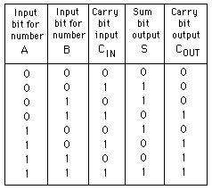
To test the full-adder bit, I'll apply every possible combination of the three inputs and see how it reacts:
In [6]:


initialize()  # Initialize for a new simulation.

# Declare input and output signals for the full-adder bit.
a_i, b_i, c_i = Wire(name='a_i'), Wire(name='b_i'), Wire(name='c_i')
sum_o, c_o = Wire(name='sum_o'), Wire(name='c_o')

# Instantiate a full-adder bit with the I/O connections.
full_adder_bit(a_i, b_i, c_i, sum_o, c_o)

# Simulate the full-adder bit operation for every possible combination
# of the a_i, b_i and c_i inputs.
exhaustive_sim(a_i, b_i, c_i)

# Show the response of the full-adder bit to the inputs.
show_text_table()
You can compare the table of values above to this full-adder truth-table to verify it's working correctly.
Just like the register, I can build a complete adder by iteratively instantiating the full-adder bit:
In [7]:


@chunk
def adder(a_i, b_i, s_o):
    '''
    Inputs:
      a_i, b_i: Numbers to be added.
    Outputs:
      s_o: Sum of a_i and b_i inputs.
    '''

    # Create a bus for the carry bits that pass from one stage to the next.
    # There is one more carry bit than the number of adder stages in order
    # to drive the carry input of the first stage.
    c = Bus(len(a_i)+1)

    # Set the carry input to the first stage of the adder to 0.
    c.i[0] = 0

    # Use the length of the a_i input bus to set the loop counter.
    for k in range(len(a_i)):

        # The k-th bit of the a_i and b_i buses are added with the
        # k-th carry bit to create the k-th sum bit and the
        # carry output bit. The carry output is the
        # carry input to the (k+1)-th stage.
        full_adder_bit(a_i=a_i.o[k], b_i=b_i.o[k], c_i=c.o[k], s_o=s_o.i[k], c_o=c.i[k+1])
I won't even try to do an exhaustive test of the adder because with eight-bit input buses, that would take $2^8 \times 2^8 = $ 65,536 simulation cycles and nobody would even look at a fraction of the output any way. Instead, I'll just check the adder's output for a few randomly-selected inputs:
In [8]:


initialize()  # Once again, initialize for a new simulation.

# Declare 8-bit buses for the two numbers to be added and the sum.
a = Bus(8, name='a')
b = Bus(8, name='b')
s = Bus(8, name='sum')

# Instantiate an adder and connect the I/O buses.
adder(a, b, s)

# Simulate the adder's output for 20 randomly-selected inputs.
random_sim(a, b, num_tests=20)

# Show a table of the adder output for each set of inputs.
show_text_table()
You can manually check the table results to see the adder is working correctly. (Remember that the adder's output is only eight bits, so it will roll over to 0 upon reaching 256. Therefore, take the $\bmod{256}$ of the sum of the inputs and compare that to the adder's output. For example, $(72 + 213) \bmod{256} = (285) \bmod{256} = 29$.)
Now I can move up another level in the hierarchy and build a counter from the adder and register:
In [9]:


@chunk
def counter(clk_i, cnt_o):
    '''
    Inputs:
      clk_i: Counter increments on the rising edge of the clock.
    Outputs:
      cnt_o: Counter value.
    '''
    # The length of the counter output determines the number of counter bits.
    length = len(cnt_o)

    one = Bus(length, init_val=1)  # A constant bus that carries the value 1.
    next_cnt = Bus(length)         # A bus that carries the next counter value.

    # Add one to the current counter value to create the next value.
    adder(one, cnt_o, next_cnt)

    # Load the next counter value into the register on a rising clock edge.
    register(clk_i, next_cnt, cnt_o)
Having finally reached the top of the hierarchy, I'll use the counter to complete the implementation of the LED blinker:
In [10]:


@chunk
def blinker(clk_i, led_o, length):
    '''
    Inputs:
      clk_i:  This is a clock signal input.
      length: This is the number of bits in the counter that generates the led_o output.
    Outputs:
      led_o:  This is an output signal that drives an LED on and off.
    '''
    cnt = Bus(length, name='cnt')  # Declare the counter bus with the given length.
    counter(clk_i, cnt)  # Instantiate a counter of the same length.

    # Attach the MSB of the counter bus to the LED output.
    @comb_logic
    def output_logic():
        led_o.next = cnt[length-1]
Let's check the operation by simulating a small LED blinker as we did in the previous example:
In [11]:


initialize()                 # Initialize for simulation.
clk = Wire(name='clk')       # Declare the clock input.
led = Wire(name='led')       # Declare the LED output.
blinker(clk, led, 3)         # Instantiate a three-bit blinker and attach I/O signals.
clk_sim(clk, num_cycles=16)  # Apply 16 clock pulses.
show_waveforms()             # Look at the waveforms.
A blinker with a three-bit counter should output an LED signal that runs at an eighth of the incoming clock frequency. The waveforms show that's what is happening.
Since the simulation seems to work, it's time to convert a larger version of the blinker into Verilog after which it can be compiled and run on an iCEstick. (Because this LED blinker uses a hierarchical description that results in a lot of smaller, individual components at the lower levels, it will take longer to generate the Verilog than the previous example. Be patient!)
In [12]:


toVerilog(blinker, clk_i=clk, led_o=led, length=22)
Out[12]:
Whew, done! You may notice a few warnings about undriven signals, but don't worry about those.
The next step is to write a file with the blinker pin assignments for the iCEstick board. The 12 MHz clock enters through pin 21 of the FPGA, and LED D1 is driven by pin 99.
In [13]:


with open('blinker.pcf', 'w') as pcf:
    pcf.write(
'''
set_io led_o 99
set_io clk_i 21
'''
    )
The following commands will compile the Verilog and pin assignments into a bitstream file:
In [14]:


!yosys -q -p "synth_ice40 -blif blinker.blif" blinker.v
!arachne-pnr -q -d 1k -p blinker.pcf blinker.blif -o blinker.asc
!icepack blinker.asc blinker.bin
Finally, the bitstream is ready to download into the iCEstick:
In [15]:


!iceprog blinker.bin
And that's it! LED D1 on your iCEstick board should be blinking. The LED blinker has been rebuilt using hierarchical design but still functions identically to the original.
After all the effort of breaking down the LED blinker into a hierarchy and then implementing it in MyHDL from the bottom up, you might ask yourself: "Was this a good idea?"
In the sense of learning about hierarchy and abstraction, yes it was. Illustrating these principles by showing how they're applied to a problem you've already solved is a time-honored technique.
But in the sense of good design practice, then the answer is NO! It took a lot more effort to get the same result that was originally expressed in a few lines of code. And less code is better code: there's fewer places to make a mistake. It's also easier to understand something that you can take in with almost a single glance versus scanning through multiple screens of code, which is important if you're trying to maintain and extend a design over a long period of time.
But real designs usually can't be solved with just a few lines of code. That's where hierarchy and abstraction can help you out. But don't carry it to an extreme: when you get to a level in the hierarchy that you can describe with a few lines of code, then don't break it down any further. Skill in any discipline is not just knowing what to do, but also knowing when not to do it.
You might also be asking: "Forgetting about code size and clarity,
is one of these designs using the resources of the FPGA more efficiently?"
We can get a feel for this by omitting the -q option when running Yosys
so it will spit out a bunch of status information as it works.
Near the end, you'll see a section that reports how much of each
type of FPGA resource was used to build the synthesized design.
These are the stats for the low-level, hierarchical LED blinker:
=== blinker ===

   Number of wires:                 65
   Number of wire bits:            191
   Number of public wires:          59
   Number of public wire bits:     185
   Number of memories:               0
   Number of memory bits:            0
   Number of processes:              0
   Number of cells:                 50
     SB_DFF                         22
     SB_LUT4                        28
The low-level blinker uses 50 cells in the FPGA: 22 for the D flip-flops (SB_DFF) of the counter and 28 four-input lookup tables (SB_LUT4) for the adder. (The iCE40HX1K FPGA on the iCEstick has 1,280 LUTs and D flip-flops, so we're not exactly straining it here.)
Compare that with the stats for the high-level, non-hierarchical LED blinker we designed in the previous example:
=== blinker ===

   Number of wires:                  5
   Number of wire bits:             68
   Number of public wires:           3
   Number of public wire bits:      24
   Number of memories:               0
   Number of memory bits:            0
   Number of processes:              0
   Number of cells:                 64
     SB_CARRY                       20
     SB_DFF                         21
     SB_DFFE                         1
     SB_LUT4                        22
The high-level design actually uses more total cells (64), but of different types. It still employs 22 D flip-flops (the SB_DFFE is a flip-flop with an enable input). It does use fewer LUTs (22 versus 28), but it makes up for that by using 20 carry logic circuits (SB_CARRY) specialized for computing the carry bits in an adder.
However, these stats are a bit misleading because the iCE40 FPGA packs a LUT, carry logic and a DFF all together in a single logic cell (LC). So the high-level blinker could possibly be packed into a total of 22 LCs, while the low-level version would require a minimum of 28 LCs (six of which would use only the LUT and leave the DFF idle).
In order to resolve the question, we can omit the -q option
for the Arachne-pnr so it will also generate some additional information.
Here's the result for the low-level blinker:
After packing:
IOs          2 / 96
GBs          0 / 8
  GB_IOs     0 / 8
LCs          28 / 1280
  DFF        22
  CARRY      0
  CARRY, DFF 0
  DFF PASS   0
  CARRY PASS 0
BRAMs        0 / 16
WARMBOOTs    0 / 1
PLLs         0 / 1
And here's the stats for the high-level version:
After packing:
IOs          2 / 96
GBs          0 / 8
  GB_IOs     0 / 8
LCs          24 / 1280
  DFF        3
  CARRY      2
  CARRY, DFF 19
  DFF PASS   0
  CARRY PASS 1
BRAMs        0 / 16
WARMBOOTs    0 / 1
PLLs         0 / 1
You can see the high-level blinker can be packed into just 24 LCs, while the low-level version requires 28 LCs.
So why is the high-level design more efficient than the low-level one?
It's because the intent of the high-level version is more obvious.
Synthesizers contain optimizers that look for common code structures like
q.next = q + 1 and realize that this implies the need for an adder and a register.
Knowing that, the synthesizer can make use of special purpose circuitry
like the carry logic.
But the low-level design doesn't expose a clear intent; it's broken down into a collection of logic gates for the full-adders and D flip-flops for the register. That's like being handed a bag of jigsaw puzzle pieces: you know there's a picture in there, somewhere, but it's a lot of work to put it all back together. The synthesizer feels the same way. And since there's nothing obvious to trigger its optimizers, it has to go with a suboptimal design that doesn't use the special purpose circuitry.
The takeaway from this: write the leaves of your hierarchy tree using high-level code statements and let the synthesizer do the low-level work from there.
Now, maybe some you have a final question: "How do bears factor into all of this?"
They don't. I can't believe I have to keep telling you that.
[1] The gate implementation of a full-adder bit is touched on in the Wikipedia article on binary adders. The minutiae involve binary arithmetic, logic minimization, and computer arithmetic circuits, all of which are discussed on many sites in much more detail than I'm willing to provide here.
[2] The Bus objects provided by PygMyHDL can be thought of as an array of Wire objects.
The function of a bus is to accept logic levels output by some circuitry and transfer it to the inputs of some
other circuitry. In order to drive a particular wire at index $k$ of a bus B, you have to access the $k$-th input
to the bus using the notation B.i[k]. Then, when you want to get hold of that value somewhere else, you
can access the output of the bus using the notation B.o[k]. So when you connect buses to a MyHDL function,
you'll use the .o suffix for a bus that is driving the function's inputs, and a .i suffix for a bus that is
receiving values from the function's outputs.
[3] If you have sharp eyes, you'll notice I don't use the .o and .i suffixes
when I connect the data_in and data_out buses to the instantiation of the register.
That's because I don't need to access individual bits at that point, therefore I can just pass the
entire bus to the register. The internals of register will use the suffixes when attaching bits of these
buses to the individual D flip-flops.